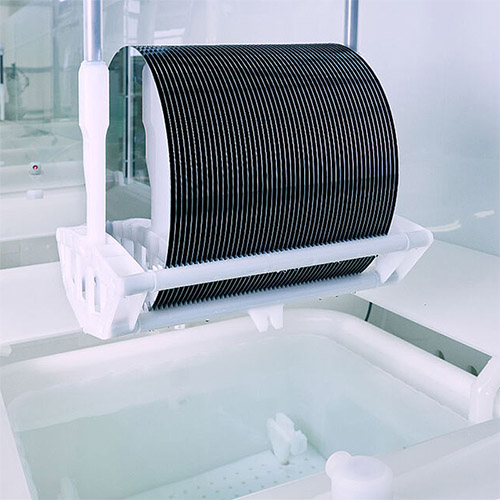
90nm and below the process mainly use 300mm semiconductor wafers, 90nm above the process mainly use 200mm or smaller size wafers; 300mm will still be the mainstream of semiconductor wafers, 12-inch semiconductor wafers can be used more than 8-inch wafers more than twice the area, the availability of (a measure of the number of chips per unit of wafers can be produced index) is 8-inch wafers of 2.25 times or so.
In addition to the common dimensional size and thickness, 300mm wafers have increased parameters such as flatness, warpage, curvature, and surface metal residue, relative to 200mm wafers, due to the requirements of advanced processes. In terms of purity, advanced process wafers require 9N (99.99999999999%) - 11N (99.9999999999999%). Semiconductor wafer core process includes single crystal process, slicing process, grinding process, polishing process, epitaxial process, etc., the degree of technological specialisation is high, of which the single crystal process is the most core technology, which determines the size of the wafer, resistivity, purity, oxygen content, dislocations, crystal defects, and other key technical indicators, in the process of single crystal growth, it is also necessary to pay attention to the temperature control and the rate of lifting and pulling and so on.


Tel:
15796350920
 XinGe SEMI